Multimedia Gallery
Using pressure to control graphene transistors
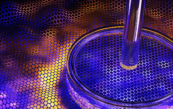
Researchers at Columbia University compressed layers of boron nitride and graphene to enhance the material's band gap, bringing it one step closer to being a viable semiconductor for use in today’s electronic devices.
More about this image
An international team of researchers led by Columbia University has developed a technique to manipulate the electrical conductivity of graphene with compression, bringing the material one step closer to being a viable semiconductor for use in today’s electronic devices.
"Graphene is the best electrical conductor that we know of on Earth," said Matthew Yankowitz, a postdoctoral research scientist in Columbia’s Physics Department and first author of the study. "The problem is that it's too good at conducting electricity, and we don't know how to stop it effectively. Our work establishes for the first time a route to realizing a technologically relevant band gap in graphene without compromising its quality. Additionally, if applied to other interesting combinations of 2D materials, the technique we used may lead to new emergent phenomena, such as magnetism, superconductivity and more."
The unusual electronic properties of graphene, a 2D material comprised of hexagonally-bonded carbon atoms, have excited the physics community since its discovery more than a decade ago. Graphene is the strongest, thinnest material known to exist and a superior conductor of electricity. The unique atomic arrangement of the carbon atoms in graphene allows its electrons to easily travel at extremely high velocity without the significant chance of scattering, saving precious energy typically lost in other conductors.
Yankowitz says scientists have been conducting experiments at high pressures in conventional 3D materials for years but no one had yet figured out a way to do them with 2D materials. Now with the new technique, researchers will be able to test how applying various degrees of pressure changes the properties of a vast range of combinations of stacked 2D materials.
The study was funded in part by U.S. National Science Foundation grants DMR 1462383, DMR 1420634 and DMR 1157490.
Learn more about this research in the NSF News From the Field story Researchers control the properties of graphene transistors using pressure. (Date image taken: unknown; date originally posted to NSF Multimedia Gallery: Aug. 10, 2018)
Credit: Columbia University Public Affairs
Images and other media in the National Science Foundation Multimedia Gallery are available for use in print and electronic material by NSF employees, members of the media, university staff, teachers and the general public. All media in the gallery are intended for personal, educational and nonprofit/non-commercial use only.
Images credited to the National Science Foundation, a federal agency, are in the public domain. The images were created by employees of the United States Government as part of their official duties or prepared by contractors as "works for hire" for NSF. You may freely use NSF-credited images and, at your discretion, credit NSF with a "Courtesy: National Science Foundation" notation.
Additional information about general usage can be found in Conditions.
Also Available:
Download the high-resolution JPG version of the image. (16.9 MB)
Use your mouse to right-click (Mac users may need to Ctrl-click) the link above and choose the option that will save the file or target to your computer.

