Multimedia Gallery
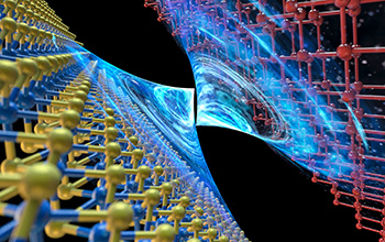
Interface between semimetal and 2D semiconductor
In this illustration, at the interface between the semimetal bismuth and the 2D semiconductor molybdenum disulfide, there is no energy barrier for an electron to go through, leading to an ultralow contact resistance between them. Researchers discovered that the semimetal, whose electronic properties fall between those of metals and semiconductors, promises a more viable alternative to silicon, which is found in most modern-day transistor technologies.
[Research supported by U.S. National Science Foundation grant DMR 1807233.]
Learn more in the Massachusetts Institute of Technology news release Advance may enable “2D” transistors for tinier microchip components. (Date of image: May 2023; date originally posted to NSF Multimedia Gallery: May 26, 2023)
Credit: Massachusetts Institute of Technology
Images and other media in the National Science Foundation Multimedia Gallery are available for use in print and electronic material by NSF employees, members of the media, university staff, teachers and the general public. All media in the gallery are intended for personal, educational and nonprofit/non-commercial use only.
Images credited to the National Science Foundation, a federal agency, are in the public domain. The images were created by employees of the United States Government as part of their official duties or prepared by contractors as "works for hire" for NSF. You may freely use NSF-credited images and, at your discretion, credit NSF with a "Courtesy: National Science Foundation" notation.
Additional information about general usage can be found in Conditions.
Also Available:
Download the high-resolution JPG version of the image. (1.1 MB)
Use your mouse to right-click (Mac users may need to Ctrl-click) the link above and choose the option that will save the file or target to your computer.

