Multimedia Gallery
Graphite-Based Circuitry
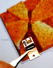
A close-up image showing a proof-of-principle graphene device against an image of graphene patterning.
More About this Image
This image was taken as part of a study of how electrons behave in circuitry made from ultra-thin layers of graphite -- known as graphene, which suggests the material could provide the foundation for a new generation of nanometer-scale devices that manipulate electrons as waves -- much like photonic systems control light waves. The research began in 2001 under Walt de Heer, a professor at Georgia Institute of Technology's School of Physics, and his team, and is supported by the National Science Foundation (NSF) and Intel Corporation. To learn more about this discovery, see the March 14, 2006, Georgia Tech press release "Carbon-Based Electronics: Researchers Develop Foundation for Circuitry and Devices Based on Graphite". (Date of Image: May 2005)
More about this Image
Graphite, the material that gives pencils their marking ability, could be the basis for a new class of nanometer-scale electronic devices that have the attractive properties of carbon nanotubes, but could be produced using established microelectronics manufacturing techniques.
Using thin layers of graphite known as graphene, researchers at the Georgia Institute of Technology, in collaboration with the Centre National de la Recherche Scientifique (CNRS) in France, have produced proof-of-principle transistors, loop devices and circuitry. Ultimately, researchers hope to use graphene layers less than 10 atoms thick as the basis for revolutionary electronic systems that would manipulate electrons as waves rather than particles, much like photonic systems control light waves.
"We expect to make devices of a kind that don't really have an analog in silicon-based electronics, so this is an entirely different way of looking at electronics," said Walt de Heer, a professor at Georgia Tech's School of Physics. "Our ultimate goal is integrated electronic structures that work on diffraction of electrons rather than diffusion of electrons. This will allow the production of very small devices with very high efficiencies and low power consumption."
Supported by NSF and Intel Corporation, the work was described March 13, 2006, at the March Meeting of the American Physical Society. Details of fabrication techniques have been reported in the Journal of Physical Chemistry.
Credit: Georgia Tech photo by Gary Meek
Images and other media in the National Science Foundation Multimedia Gallery are available for use in print and electronic material by NSF employees, members of the media, university staff, teachers and the general public. All media in the gallery are intended for personal, educational and nonprofit/non-commercial use only.
Images credited to the National Science Foundation, a federal agency, are in the public domain. The images were created by employees of the United States Government as part of their official duties or prepared by contractors as "works for hire" for NSF. You may freely use NSF-credited images and, at your discretion, credit NSF with a "Courtesy: National Science Foundation" notation.
Additional information about general usage can be found in Conditions.
Also Available:
Download the high-resolution JPG version of the image. (3.5 MB)
Use your mouse to right-click (Mac users may need to Ctrl-click) the link above and choose the option that will save the file or target to your computer.

